Logic Drive
Introduction
We are inventing a technology based on a standardized commodity logic drive in a multi-chip package with plural standardized commodity FPGA IC chips and one or plural non-volatile memory IC chips for use in varieties of applications requiring logic, computing and/or processing functions by field programming.
Uses of standardized commodity logic drives are analogous to uses of standardized commodity data storage devices, such as solid-state disk (drive), data storage hard disk (drive), USB drive or stick. It differs in that standardized commodity data storage devices have memory functions for data storage, while standardized commodity logic drives have logic functions for processing and/or computing. Uses of standardized commodity FPGA IC chips are analogous to uses of standardized commodity data storage memory IC chips, such as standard commodity DRAM chips or standard commodity NAND flash chips, and differs in that the latter has memory functions for data storage, while the former has logic functions for processing and/or computing.
The disruptive concept: Software-Defined Hardware
We are inventing a logic drive to inspire innovation and lower the barrier for implementing innovations in IC chips designed and fabricated using an advanced IC technology node or generation.
An innovator with an innovation or an application concept may purchase the standardized commodity logic drive and write software programming to load into the standardized commodity logic drive to implement their innovation or application concept including algorithms or architectures of computing, processing, learning and inferencing.
Innovators may program the logic drive by writing software programs to implement their innovations or applications using a common programing language such as Java, C++, Matlab, Assembly Language, Pascal, Python, Visual Basic, PL/SQL or JavaScript language.
Creating a new Public Innovation Platform
In the early 1990’s, innovators could design IC chips and fabricate IC chips in a semiconductor foundry fab using technology nodes of µm-scale at the cost of several hundred thousands US dollars. The IC foundry fab was then known as the “Public Innovation Platform”.
The Public Innovation Platform revolutionized the electronic/semiconductor industry. With the availability of the Public Innovation Platform, innovative and talented IC design engineers rushed to found fabless logic IC design companies in the 1990's. Among them, many succeeded and have become significant and influential semiconductor companies; and some even become the top ten semicondutor companies worldwide in 2018. All of the top ten semiconductor companies worldwide in 1995 were integrated design (IDM) companies. Among them, only one survives as an logic IDM company and is still listed in the top ten seminconductor companies worldwide in 2018; all the others turned into fabless logic semiconductor companies. The Public Innovation Platform even enabled the birth of the first generation of truth smart phones in 2007 which completely changed the lives of human beings.
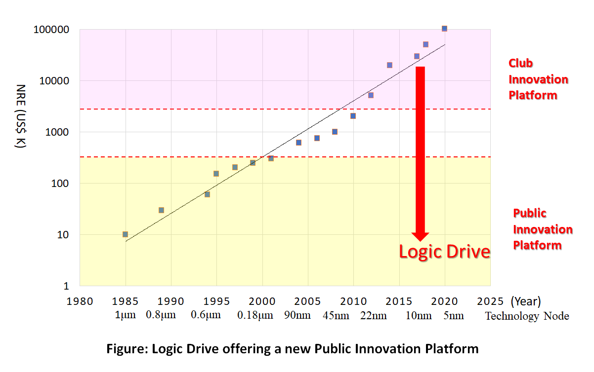
However, when IC technology nodes advanced to less than 20 nm, only a few giant system houses or IC design companies could afford to use such semiconductor foundry fab as the cost to develop and implement an IC chip using these advanced technology nodes was over US $20M. As a result, the semiconductor foundry fab has become a “Club Innovation Platform” for club innovators only. (See Figure) The Club Innovation Platform is now inviting giant system or service companies, armed with their rich finances and huge markets, to jump into designing their own semiconductor chips. These giant system or service companies become dominant club members of the current Club Innovation Platform.
Our technology offers a new “Public Innovation Platform” allowing innovators to easily and cheaply implement or realize their innovation or application in semiconductor IC chips with advanced technology nodes less than 20 nm by using the standard commodity logic drives and writing software programs using common programing languages. The innovators can use their own commodity logic drives or rent logic drives from data centers or clouds through networks.
Lowering the barrier for innovation
In the current implementation of an innovation or application by developing an ASIC or COT IC chip, the NRE cost increases to greater than US $20M or even exceeding US $100M, or US $200M using advanced technology nodes less than 20 nm. The cost of a photo mask set for an ASIC or COT chip at the 16 nm technology node or generation may be over US $5M.
Using the standardized commodity logic drive may greatly reduce the NRE cost. For example, for the same or similar innovation implement in an ASIC or COT IC chip, using the standard commodity logic drive may reduce the NRE cost down to less than US $1M. (see Figure)
New business model- Creating a standard commodity logic IC industry
Our technology provides a method to change the current ASIC or COT logic IC chip industry/business into a commodity logic IC chip industry/business, just like the current commodity DRAM, or commodity NAND flash memory IC chip industry/business.
The current ASIC or COT logic IC chip design and manufacturing companies (including fabless IC design and product companies, IC foundry or contracted manufacturing companies, integrated design manufacture companies (IDM)) may become companies with the following business models:
- designing, manufacturing, and selling the standard commodity FPGA IC chips similar to the current commodity DRAM or flash memory chip industry/business;
- designing, manufacturing, and selling the standard commodity logic drives similar to the current commodity DRAM or flash memory module industry/business.